

The Vanderbilt Institute for Space and Defense Electronics (ISDE) will lead an international team of researchers investigating how radiation affects 3D electronics and systems under a three-year $3 million federal project.
The team includes world-leading research and development groups in 3D integrated circuit technologies in both industry and academia. The basic research grant, from the Defense Threat Reduction Agency, an arm of the U.S. Department of Defense, is $1 million a year for three years with a two-year renewable option and could total $5 million.
As industry looks to enhance the performance and capabilities by building up – producing stacked, three-dimensional electronics – the work has significant implications beyond classic national defense research. Space-based electronics are core components of communication systems, supporting near global adoption of mobile devices, and will become more vital to Internet of Things applications, from medical implants to smart appliances, autonomous vehicles and entire automated buildings.
“After more than 50 years of shrinking integrated circuits to continually make more capable and portable devices, the bottleneck is now in the integration of different functions, often made in different technologies,” said ISDE Associate Director Mike Alles, a research professor in electrical engineering and computer science and principal investigator of the new project.
Three-dimensional integration dramatically reduces the size and weight of electronics. It also eliminates the significant power consumption and signal slowdown of conventional chip-to-chip electronic connections on circuit boards, making 3D configuration attractive for many commercial, military, and space applications.
“These types of integrated structures are relatively new and still developing, so there is a lot of interest in understanding the associated reliability implications. In our case for this grant, the focus is radiation the devices might be exposed to in a space or military environment, or perhaps even certain medical applications,” Alles said.
The project is entitled RER-3D: A Research Center for Radiation Effects Reliability Mechanisms Unique to 3D Integration and will be under ISDE’s direction.
Vanderbilt already has the world’s largest university-based program in radiation effects on microelectronics. ISDE was established in 2003 specifically to support the needs of government and industry for engineering expertise in radiation interaction with electronics. The institute and the existing Radiation Effects Research group together have five fulltime engineers in addition to 13 faculty members and 25 graduate students.
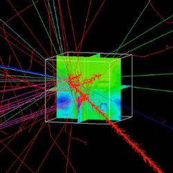
The effects of radiation in the layered devices themselves won’t necessarily be novel. But the nature of three-dimensional circuitry introduces new paths through which the radiation travels on the way to the specific layers. This may shield or enhanced the effects and also introduces the potential for more, simultaneous errors due to a single radiation particle.
“This complicates the process because each layer is seeing a bit of different radiation environment locally,” Alles said. “Modeling and simulation will play a key role in analyzing these effects.”
ISDE specializes in use of modeling, simulation and testing to characterize such effects on materials, devices, circuits and systems. This project builds on Vanderbilt’s substantial history of studying the effects of radiation and the response of circuits.
When combined with the radiation transport modeling, the results can be used to predict how 3D integrated devices will respond.
Novel experimental techniques also will be applied to investigate the unique considerations of radiation effects in 3D integrated technologies and to calibrate and validate models.
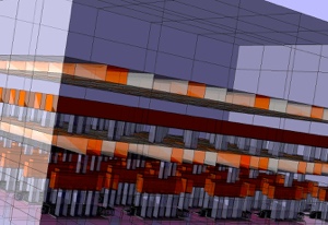
Three-dimensional (3D) integration of electronic, optical, and electro-mechanical functions improves performance-to-power ratios and shrinks physical footprints. Much like building in a crowded, popular downtown, electronics gain valuable real estate by growing vertically.
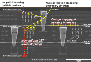
And layers have different degrees of integration, just as an all-residential high-rise would have different power, space and insulation requirements than a mixed use development with floors of retail space. The level of integration also will influence how 3D electronics exposed to radiation behave. A more intimate connection between functional chips enhances signal performance but also could increase likelihood of failure in extreme conditions such as space. For example, radiation-induced charge could become trapped at interfaces where layers are attached together and cause degradation or failure.
ISDE’s research partners include top international commercial/industry technology research labs and university programs. Among them:
- Imec, an international research and innovation hub in nanoelectronics and digital technologies, which has a track record in 3D technologies, process development, and reliability programs;
- Cea-LETI, the technology research unit of the French Atomic Energy and Alternative Energy Commission, which existing programs in 3D integration and will provide test structures and devices from their state of the art process line;
- University of California-Los Angeles and North Caroline State University, which are top institutions in the design and construction of vertically integrated circuits;
- Nhanced Semiconductors, a commercial leader in deployment of 3D technologies;
- Aerospace Corporation, which, with Vanderbilt, has expert capability to study how radiation travels through objects and how objects respond.
The new research center also creates opportunities for undergraduate and graduate student research. Internships with industry and university partners are planned, as is collaborating with other agencies across DoD and NASA.
“The Center concept in the title really arose because we saw many common interests underlying the broader, more application-specific reliability spectrum here,” Alles said. “We believe we have a solid core team across the seven organizations, and are exploring collaborating with other organizations where there are common interests.”
This work is supported by a federally funded Basic Research Grant, No. HDTRA1-18-1-0002.
Media Inquiries:
Pamela Coyle, (615) 343-5495
Pam.Coyle@Vanderbilt.edu
Twitter @VUEngineering